Photoresist Barriers
Photoresist Barriers – Spray Coating Photoresist – Cheersonic
1. Exploring Lithography: From Printing
Lithography is a process technology that uses the principle of photochemical reaction and chemical and powerless etching methods to transfer the pattern on the reticle to the wafer. The principle of lithography originated from photoengraving in printing technology. Unlike printing, the lithography process does not use ink as a medium, but completes the transfer of this information with the help of the chemical changes of photosensitive substances after being exposed to light (exposure). .
Lithography technology is mainly divided into optical lithography and particle beam lithography according to the exposure light source (common particle beam lithography mainly includes X-ray, electron beam and ion beam lithography, etc.). Among them, optical lithography is the most important lithography technology at present, and it will still occupy the mainstream position in the next few years.
Under the guidance of Moore’s Law, optical lithography has undergone changes in exposure methods such as contact/proximity, equal-magnification projection, reduced stepper projection, and step-and-scan projection. As the size of integrated circuit devices continues to shrink, the computing speed and integration of chips continue to increase, and higher requirements are placed on the exposure resolution of lithography technology.
2. Introduction to photoresist: a technology-intensive industry
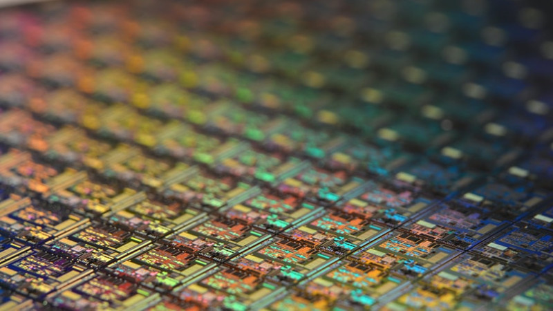
Photoresist, also known as photoresist, refers to a resist etching film material whose solubility changes through irradiation or radiation of ultraviolet light, electron beam, ion beam, X-ray, etc. Photoresist is currently widely used in the processing and production of fine pattern circuits in the optoelectronic information industry, accounting for about 6% of the total IC manufacturing material market, and is an important semiconductor material. Photoresist is the material with the highest technical barriers in electronic chemicals, and has the characteristics of high purity requirements, complex production process, and long technology accumulation period.
3. Photolithographic Collagen Materials
Photoresist is composed of film-forming resin (polymerization agent), photoinitiator, solvent and additives. The film-forming resin is used to aggregate different materials in the photoresist together to form the skeleton of the photoresist, which determines the basic properties of the photoresist, such as hardness, flexibility, and adhesion. Photoinitiators, including photosensitizers and photoacid generators, are the key components of photoresist and play a decisive role in the sensitivity and resolution of photoresist.
Solvent is the largest component in photoresist, the purpose is to keep the photoresist in a liquid state, but the solvent itself has little effect on the chemical properties of the photoresist. Additives include monomers and other auxiliaries, etc. The monomers have a regulating effect on the photochemical reaction of the photoinitiator, and the auxiliaries are mainly used to change the specific chemical properties of the photoresist.
The data shows that resin accounts for 50% of the total cost of photoresist, and it accounts for the largest proportion of photoresist raw materials, followed by monomers accounting for 35% and photoinitiators and other auxiliaries accounting for 15%. For high-end photoresists, resin accounts for a higher proportion of the cost.
4. Equipment required for photoresist inspection and production
Since different semiconductor photoresists are different in terms of applicable wavelengths, formulations, and quality of raw materials, their production equipment and testing equipment are also different.
The reactor is the main photoresist production equipment, the g/i line photoresist production equipment is a stainless steel reactor, and the KrF and ArF photoresists are fluorine-lined reactors.
The inspection equipment involved in the ArF photoresist project includes lithography machine, CDSEM, glue developing machine, bright field defect scanner, defect analysis equipment, gas particle analyzer, etc.
5. Photoresist classification: positive photoresist and negative photoresist
According to the chemical reaction mechanism, photoresists can be divided into two categories: negative photoresists and positive photoresists. Both are widely used in PCBs, panels, and semiconductors. However, due to the easy deformation and expansion of negative photoresists during development, the resolution is usually only 2 microns. Therefore, the application of positive photoresists is more popular, accounting for The total amount of photoresist is more than 80%. ArF photoresist and EUV photoresist are basically positive photoresist. Positive photoresist refers to the photoresist that in the photolithography process, after the coating is exposed and developed, the exposed part is dissolved in the developing solution and the unexposed part remains to form an image. Negative photoresists are the opposite of positive photoresists, where the unexposed parts are dissolved and the exposed parts form the image.
6. Overview of photoresist technical barriers
Photoresist is the material with the highest technical barriers in electronic chemicals, and has the characteristics of high purity requirements, complex production process, large investment in production and testing equipment, and long technology accumulation period. From the perspective of related technologies, the core technology of photoresist includes formulation technology, quality control technology and raw material technology. Formulation technology is the core of the realization of photoresist functions, and quality control technology can ensure the stability of photoresist performance. The quality of the photoresist material plays a key role in the quality of the photoresist.
7. Photoresist customer barriers: extremely high barriers and long certification cycles
In terms of photoresist, according to industry practice, photoresist products are generally verified and factory (production line) qualifications are verified before photoresist is supplied. Among them, photoresist verification is divided into PRS (photolithography) according to the verification stage. Adhesive performance test), STR (small test), MSTR (batch verification) and Release (passed verification); in terms of factory (production line) qualification verification, mainly in the quality system, supply stability, factory (production line) capacity, etc. aspects are verified. After the factory (production line) qualification verification and product verification pass, the official supply to customers can be realized. The verification period is usually 6-24 months.
The main process of photoresist monomer verification is: the manufacturer sends samples to potential customers for R&D samples, and the customer tests various quality indicators and synthesizes the resin for verification; after the product verification is passed, the factory inspection quality system certification is carried out; finally, the pilot test is carried out. Level product order verification. The photoresist monomer verification cycle is usually 6-24 months.
The ultrasonic coating system can use advanced layering technology to precisely control the flow rate, coating speed and deposition amount. Low-speed spray forming defines an atomizing spray as a precise, controllable pattern, avoiding excessive spraying when producing very thin and uniform layers. It turns out that direct spraying using ultrasonic technology is a reliable and effective way to deposit photoresist on 3D microstructures, thereby reducing equipment failures caused by excessive metal exposure to etchant.
Ultrasonic spray systems have proven to be suitable for a variety of applications that require uniform, repeatable photoresist or polyimide film coatings. Cheersonic’s coating system can control thicknesses from sub-micron to more than 100 microns, and can coat any shape or size. It is a feasible alternative to other coating technologies such as spin coating and traditional spray coating.
Cheersonic’s non-blocking ultrasonic coating technology is known for its ultra-thin micron-layer coatings of functional and protective materials. The ultrasonic vibration of the nozzle effectively dispersed the particles in the suspension and produced a very uniform particle dispersion in the film layer, while the conductive particles did not settle out of the suspension.